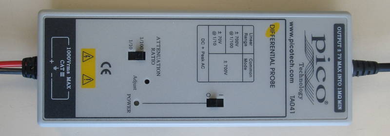
The TA041 probe, without its yellow jacket
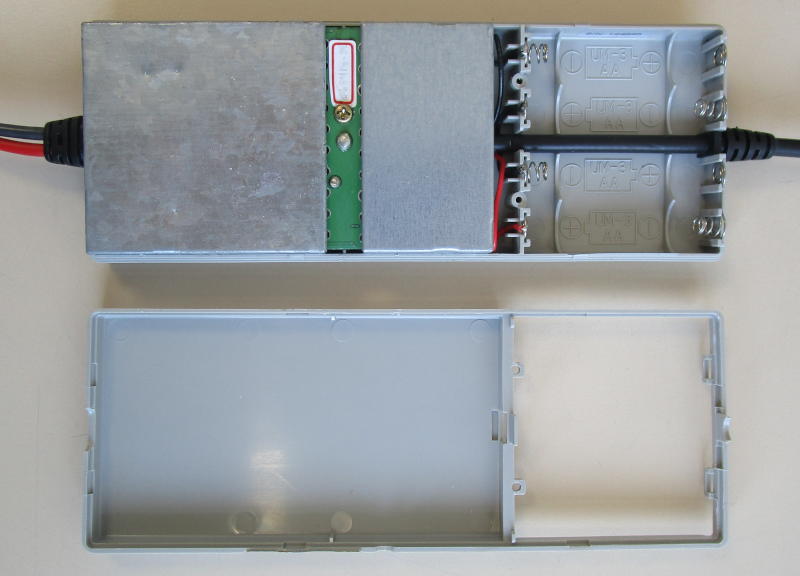
Output BNC cable is going thru batteries (also, nice hand-written serial label)
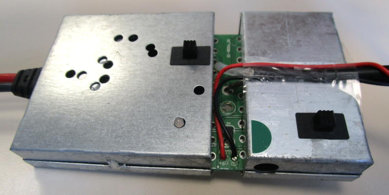
Once the plastic case opened, we can see two separate shielding enclosures. The left one is containing the analog circuits, and has multiples holes for adjusting. Not all holes are having an adjustable pot or cap behind. Maybe used for several probe versions?
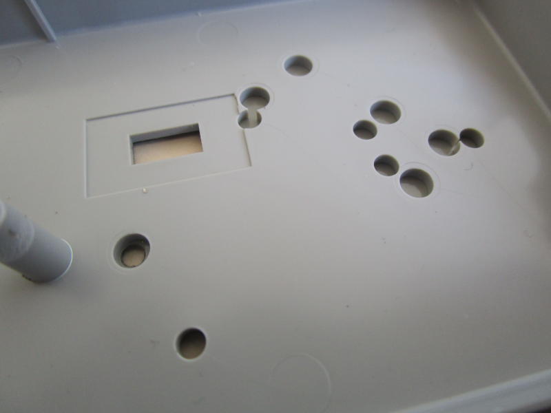
The front plastic shell halve is also having a good number of holes. Only one is not covered by the adhesive plastic sheet and allowed to be touched by the end user (if we exclude the ones for switchs and led of course).
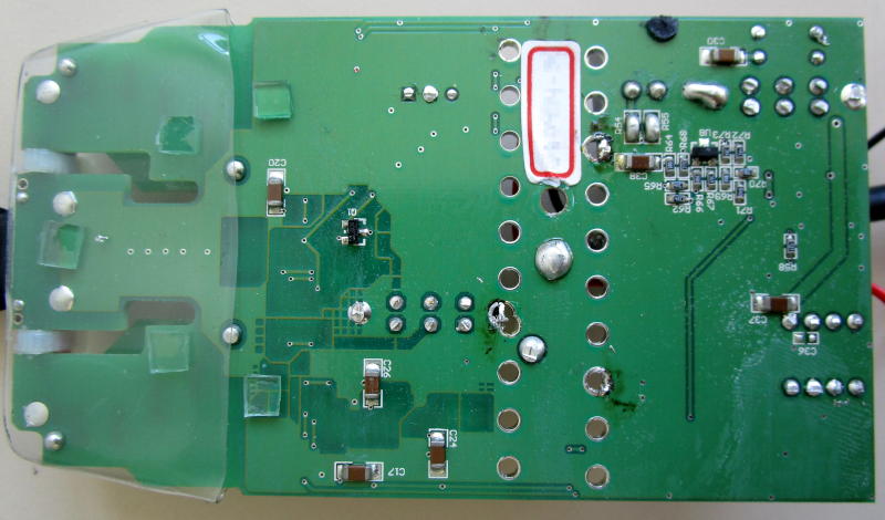
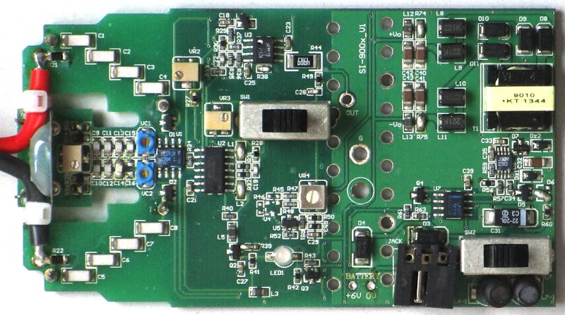
Printed circuit board bottom view, shields removed
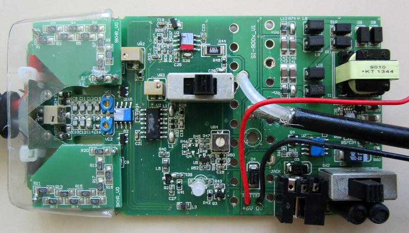
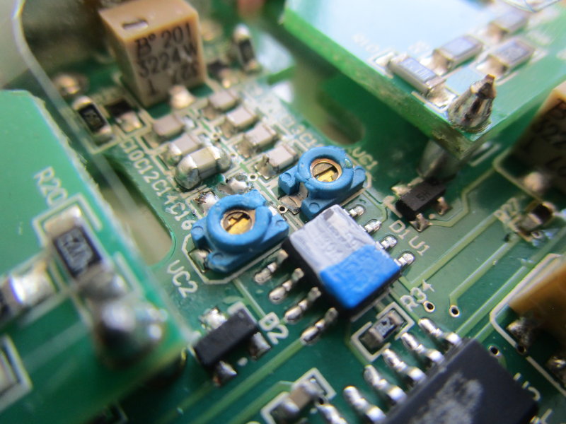
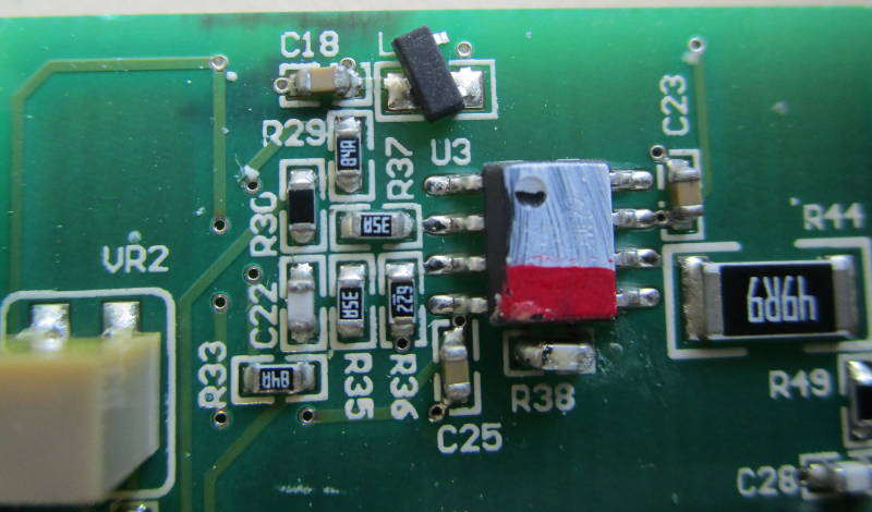
Printed circuit board top view, shields removed. Input divider in two boards, and three ICs are painted (but for what purpose?)
| Label | IC before paint removal | After paint removal | Markings | What this thing probably is |
|---|---|---|---|---|
| U1 | 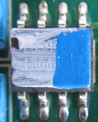 | 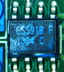 | LS591B F 1304 C | Wideband, High Gain, Monolithic Dual, N-Channel JFET |
| U2 | 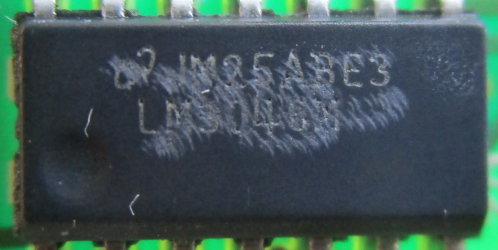 | JM25ABE3 LM3046M | NPN Bipolar Monolithic Transistor Array | |
| U3 | 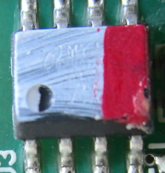 | 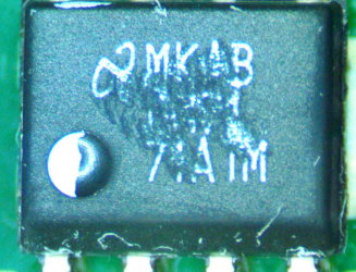 | MKAB ???? 74A IM | Op-amp |
| U4 & U5 | 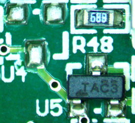 | TAC3 | Programmable Zener (U4 not populated) | |
| U6 | 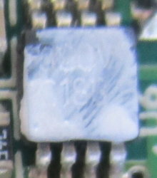 | 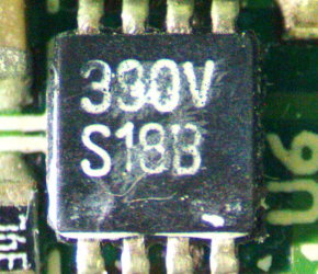 | 390V S18B | Step-up PWM DC/DC Converter |
| U7 | 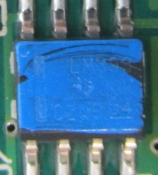 | 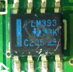 | LM393 39K C2Q5 S4 | Low Offset Voltage Dual Comparators |
Top, with input resistances boards removed (capacitive divider exposed) and ICs paint cleaned.
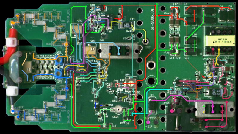
Reversing the boards, both sides...
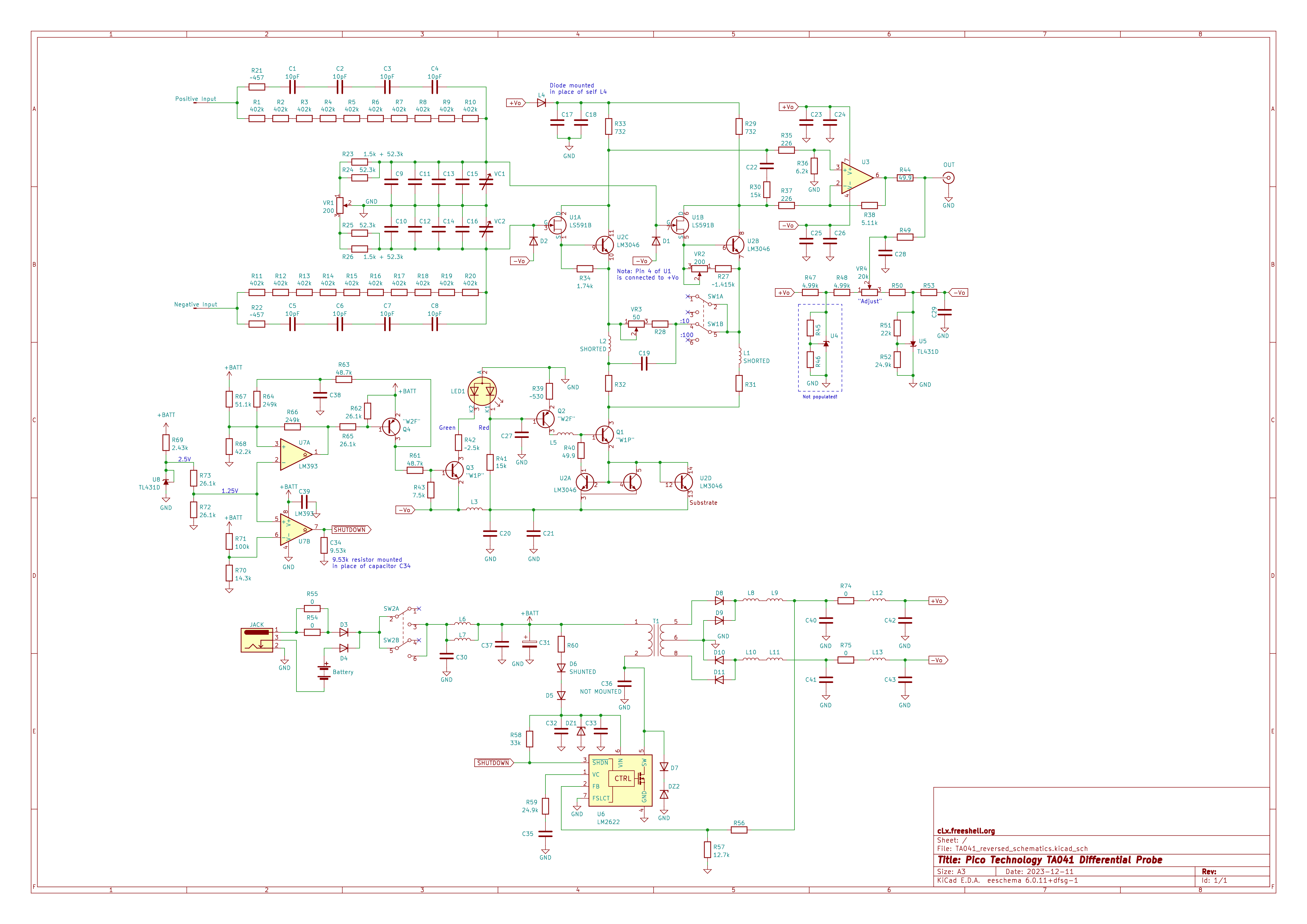
Reversed schematics. Click to enlarge!
I had to desolder a HV input capacitor from its string to measure it as a 10pF. After the divider, for each input: ~330pF//26.2kΩ to ground, measured at 10kHz. There is a lot of strange squirks in that device, like two components placed on the same SMD footprint (for both serials or parallels combinations), or replacements (diode mounted in place of an inductor, resistor in place of a capacitor, solders points in place of resistors... etc.). And, of course, some components just aren't populated.
| Labels | Marking | Value | Labels | Marking | Value |
|---|---|---|---|---|---|
| R1..R20 | 4023 | 402kΩ | R45,R46 | (not populated) | (infinite) |
| R21,R22 | (NM) | 457Ω | R47,R48 | 68B | 4.99kΩ |
| R23,R26 | 1501 + (NM) | 53.86kΩ | R49 | ||
| R24 | (NM) | R50 | |||
| R25 | (NM) | 52.13kΩ | R51 | 223 | 22kΩ |
| R27 | (NM) // ? | R52,R59 | 39C | 24.9kΩ | |
| R28 | (NM) | R53 | |||
| R29,R33 | 84A | 732Ω | R54,R55,R74,R75 | (solder point) | (zero) |
| R30 | (NM) | R56 | |||
| R31 | (NM) | R57 | 11C | 12.7kΩ | |
| R32 | (NM) | R58 | 333 | 33kΩ | |
| R34 | 24B | 1.74kΩ | R60 | (NM) // ? | |
| R35,R37 | 35A | 226Ω | R61,R63 | 67C | 48.7kΩ |
| R36 | 622 | 6.2kΩ | R62,R65,R72,R73 | 41C | 26.1kΩ |
| R38 | ? // C | R64,R66 | 39D | 249kΩ | |
| R39 | 84B // ? | 7.32k // ? | R67 | 69C | 51.1kΩ |
| R40 | 68X | 49.9Ω | R68 | 61C | 42.2kΩ |
| R41 | R69 | 38B | 2.43kΩ | ||
| R42 | R70 | 16C | 14.3kΩ | ||
| R43 | 85B | 7.5kΩ | R71 | 01D | 100kΩ |
| R44 | 49R9 | 49.9Ω | C34 | 95B | 9.53kΩ |
Resistors values. Not all. Most aren't marked and I desoldered only some for measurements...
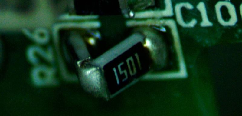
1.5k resistor added in serie with 52.3k (for fine tuning?). This is the kind of thing you don't see everyday in a marketed product...
Closeup on the input divider section, low sides. One capacitor is mounted on top of another and not on its own footprint. But why?
SOT23 diode mounted in place of an inductor named L4