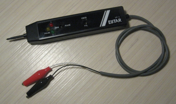
Less than $10 logic probe
This "Eistar LP-1" logic probe seems to be a very common probe, and doing its job. I accidentally damaged mine, as I connected once the supply in reverse (oops!). It was still partially working, but only in TTL levels settings, and the green "0" LED was still lit. Before repairing it, I wanted to make the schematics of it. There are two screws under the large black top sticker.
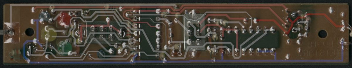
Reverse-engineering the printed circuit board...
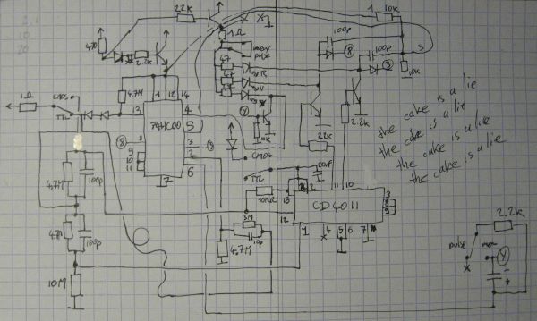
... and the somewhat long process to sketch its schematics, track after track
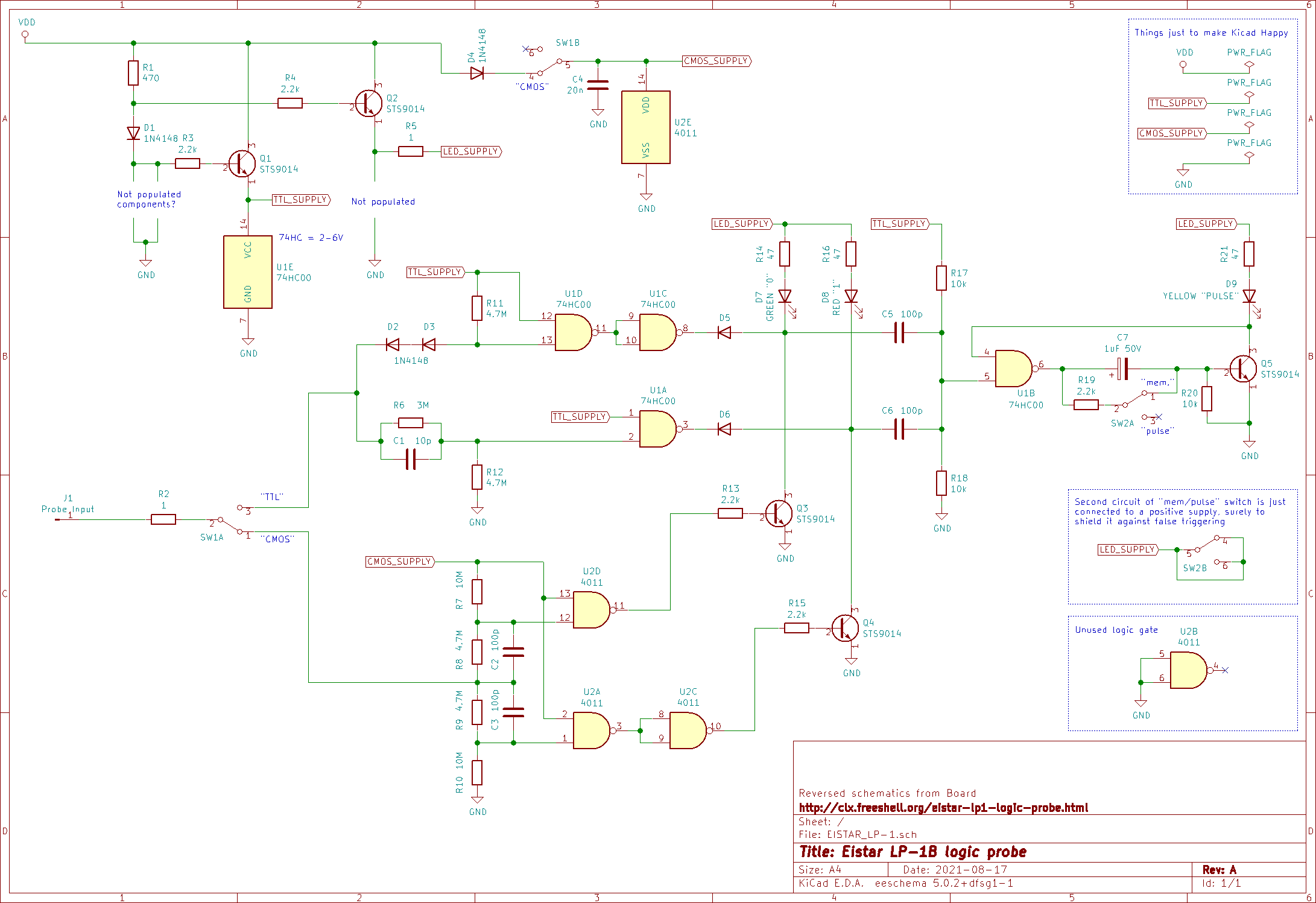
The proper Eistar LP-1 schematics (click to full size PNG)
The signal paths in CMOS mode and TTL mode are distinct. By the way, both ICs are CMOS, but the 74HC00 is for TTL levels thresholds, while the 4011 is for CMOS thresholds. The 1Ωresistors are simply used as jumpers.
And now (with a couple of measurements) it was easy to diagnose the 74HC00 as damaged (I guess it been damaged when the GND was connected to 5V and there is no protection against probing a negative voltage). Cutting 1, 3, 4, 8, 12 and 14 of U1 and the probe is reacting correctly when in CMOS settings (but no pulse indication of course).
Some vendors claims this logic probe can be powered up to 18V max, but it lacks a least a zener diode to not to supply the 74HC00 more than 5V (6 max). So I soldered a 5.6V zener diode and a 10µF capacitor on unpopulated pcb pads, powering "TTL_SUPPLY" with 5.06V. For limiting LED_SUPPLY, I also had to replace Q2 which was partially damaged too (if VDD = 10V and all LEDs off: Ve = 9.99V without the zener, 8.76V with it, and after Q2 change, 6.1V).
For protecting U1 (the 74HC00) in the future in case touching voltage more negative than ground, I added a supplementary 1N4148 diode, anode connected to ground, and cathode to the netbetween D2 and D3, and replaced R2 (a jumper resistor) by 100Ω to limit the current. Lets hope it will not reducing the bandwitch too much, and protect U1. Still, I soldered a socket...
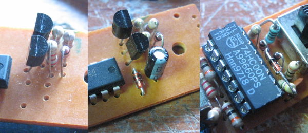
Left: unpopulated pads. Center: Zener and capacitor added on it. Right: New IC with socket, added a clamp diode to ground, and R2 changed to 100Ω.